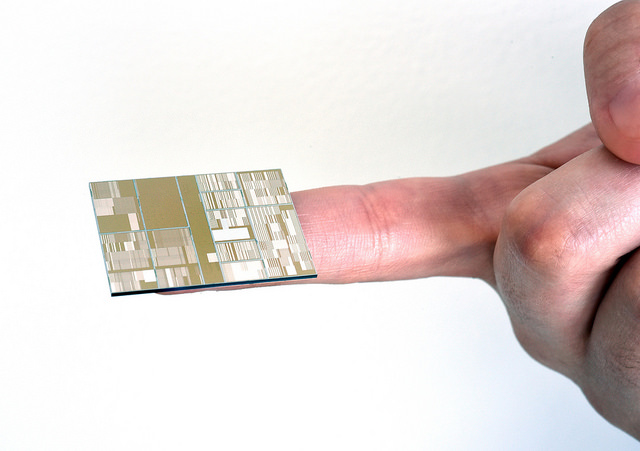
IBM announced in New York on Thursday that it has made a computer chip that contains 7-nanometer transistors. These are the smallest chips ever manufactured by any computer company so far.
According to Larry Rulison of Albany Times Union, the chips were made at IBM's 300 mm wafter manufacturing facilities at SUNY Polytechnic Institute in Albany. The new chips could go twice as fast as today's most advanced chips on the market.
"Albany played a critical role in the milestone," IBM spokeswoman Christian Vu said. "We intend to incorporate 7-nm into the road maps for IBM systems in the future."
Rulison reported that companies like IBM can pack 20 billion transistors on such a chip; in comparison, a strand of DNA is about 2 nm wide. The CEO of Silicon Valley-based VLSI Research, Dan Hutcheson, told Rulison that IBM has proven the theory behind Moore's Law, which contends that the computer industry could double the number of transistors on a chip every two years.
"Many have been predicting that it was over and that 7-nm was dead," Hutcheson said.

According to Rulison, the 7-nanometer IBM chip was made by the IBM research alliance, which included researchers from GlobalFoundries, Samsung and SUNY Poly's Colleges of Nanoscale Science and Engineering. The computer company pledged to spend $3 billion on chip technology advances over a five-year period.
"It demonstrates that they are doing what they said they would do when they sold their chip manufacturing operations to GlobalFoundries, and that they are continuing to be a research and development powerhouse in the semiconductor industry," Hutcheson said.
Steven Shankland of CNET reported that IBM used various technologies to get the prototype chip down to 7 nm. He noted that the two most important technologies used in making it included a chemical compound known as silicon germanium and "an optical etching technology using extreme ultraviolet light."
"Computer chips are built on a disk-shaped substrate of silicon crystal called a wafer, but chipmakers have long fiddled with the wafer's exact chemical composition," Shankland wrote. "Doing so can mean better electrical properties for transistors, the tiny on-off switches that in their millions or billions make up a modern microchip."
Shankland elaborated on the importance of using extreme ultraviolet light in manufacturing the chip. This process is used "for the etching of circuitry patterns on the silicon wafer."
"This etching process, called photolithography, shines light through a mask that has an extremely complicated arrangement of transparent and opaque areas," Shankland wrote. "Where the light shines or doesn't changes the composition of the wafer, which means different types of materials can be added removed to manufacture the three-dimensional transistors and interconnection circuitry."
According to Shankland, the development of the 7 nm chip could lead to devices such as "powerful smartwatches or perhaps augmented-reality contact lenses." However, semiconductor analyst Pat Moorhead of Moor Insights & Strategy of Austin, Texas, cautioned that mass production of 7-nanometer chips is still far off for now; Rulison reported that IBM no longer owns any chip factories.
"It's about research," Moorhead said. "It's a really positive thing, but there are literally 500 things that need to happen between the research and then to mass produce millions of these chips at a low cost."
Moorhead speculated that Intel, the dominant leader in making computer chips, probably has a 7-nanometer chip as well, although the company hasn't officially announced anything from that front. According to Rulison, he had doubts that IBM would overtake Intel after dominating the market of chip technology for 20 years.
"They (Intel) just don't want to tell anyone about it," Moorhead said.


